Measure with confidence — discover more.
PolarTip · high aspect ratio SiC AFM probes.
Explore the product line and pilot opportunities.
Tiny Infinities — silicon carbide AFM probes and nanoscale sensing.
Tiny Infinities develops measurement tools for semiconductor development and scientific research. Our expertise combines advanced silicon carbide nanofabrication with Raman polaritonics—an approach to sensing the infrared optical properties of nearby materials using visible light.
SiC AFM probes for demanding surfaces.
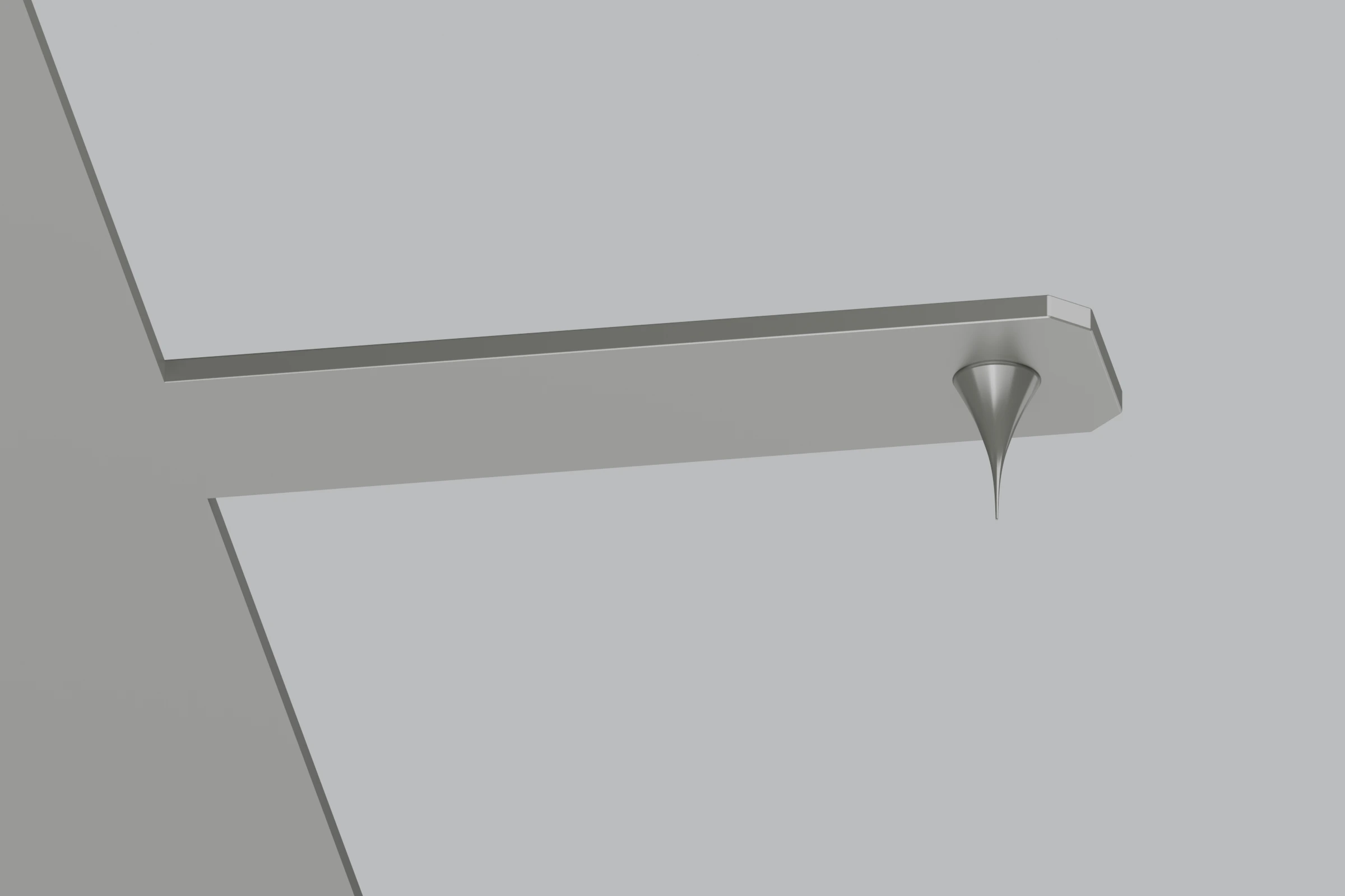
PolarTip is our silicon carbide probe line for atomic force microscopy. It brings our fabrication expertise to the challenges of feature access, tip wear and faster scanning.
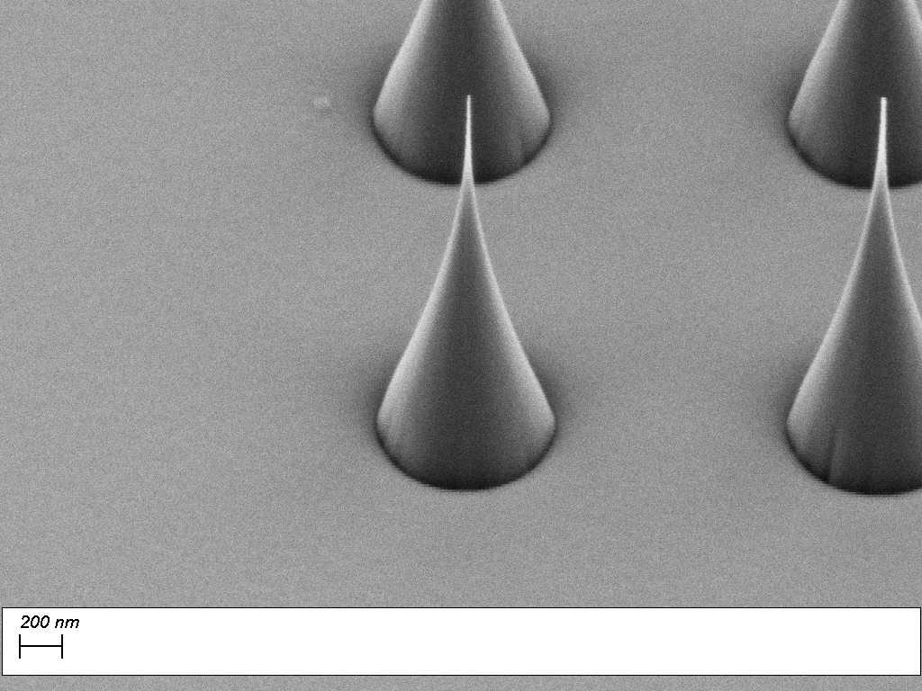
Measured 5 nm apex radius
High aspect ratio
Circularly symmetric SiC tips
Access fine, narrow features
A sharp apex and high aspect ratio address the challenge of reaching narrow surface features. Match the tip profile to the details you need to measure.
Preserve useful tip geometry
Tip wear can change apparent feature dimensions. PolarTip is designed around wear resistance to support consistent measurements over repeated scans.
Increase AFM throughput
PolarTip probes are being developed for faster scanning and higher AFM throughput, by combining SiC’s stiffness with resistance to wear and breakage.
Work with us on a PolarTip pilot, with specifications and geometry shaped around your AFM setup and measurement needs.
Understand surfaces through each process step.
Semiconductor and thin-film development
Understand how polishing, deposition and etching change a surface. We develop probes for higher-throughput AFM, combining faster-scanning research with designs intended to retain useful tip geometry.
AFM research and shared facilities
Make more of your instrument time. PolarTip is designed to preserve fine-feature access through repeated scans, with the aim of reducing interruptions caused by tip wear.
Bring SiC probe technology into your next AFM system. We collaborate on probe geometry and mechanical response to support faster scanning and meet your instrument’s integration needs.
Advanced nanofabrication in silicon carbide.
Silicon carbide is hard and chemically resistant, making it valuable for demanding applications and challenging to shape precisely. We fabricate advanced nanoscale structures in SiC and develop them into measurement tools.
PolarTip is our first product built on this expertise. We also welcome selected collaborations on SiC structures for measurement and sensing.
New ways to measure thin films.
Alongside PolarTip, we are exploring Raman polaritonics for thin-film measurement. This work underpins PolarSense, a future product direction for optical sensing shaped with semiconductor teams and research partners around their materials and measurement questions.
Engineered SiC nanostructures provide the sensing element. Visible-light Raman readout reveals how their response changes with the material nearby.
Research and engineering, brought together.
Based in Gothenburg, our team combines nanophotonics, nanofabrication, engineering and commercial development. Our work grew from research and entrepreneurship at Chalmers.
Timur Shegai
Nanophotonics & scientific direction
Betül Küçüköz
Nanofabrication & experimental research
Viktor Turnsek Dahllöf
Engineering & customer applications
Selena Krivić
Commercial development & partnerships
Discuss your
measurement challenge.
Talk to us about a PolarTip pilot or a sensing-system collaboration. Tell us what you need to measure, the setup you use and what limits your current approach.