TECHNOLOGY

Silicon carbide,
engineered for measurement.

We engineer silicon carbide nanostructures for surface measurement and optical sensing, combining materials research, precision fabrication and mechanical design.

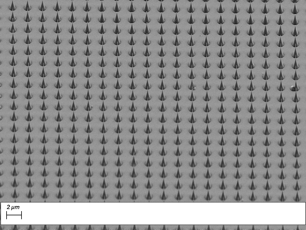
Electron micrograph of an ordered array of silicon carbide tips, with a 2 micrometre scale bar.
Array of fabricated SiC tips. Electron micrograph; scale bar: 2 µm. Select to enlarge.

01 / THE MATERIAL

Why silicon carbide?

Silicon carbide combines hardness, chemical resistance and thermal stability with an optical response shaped by its crystal structure. We engineer its geometry and fabrication process around the mechanical or optical interaction a measurement needs.

Optical access

Suitable single-crystal SiC can transmit light to sensing structures on its opposite face. Crystal selection, thickness and wavelength determine the usable optical path.

Hardness

SiC’s hardness is one reason we are developing AFM tips in this material. Useful tip life also depends on the sample, contact conditions and geometry.

Chemical resistance

Chemical resistance matters when a structure contacts different samples or environments. It also makes controlled etching a central fabrication challenge.

Thermal stability

Thermal stability supports processing and experiments at elevated temperatures. The complete structure, interfaces and surrounding system determine usable conditions.

SiC and GaN research.

Our team’s Raman-polaritonics research also examines gallium nitride (GaN) nanostructures. SiC nanofabrication remains our core project capability; the wider research helps us understand how geometry and material choice affect optical response.

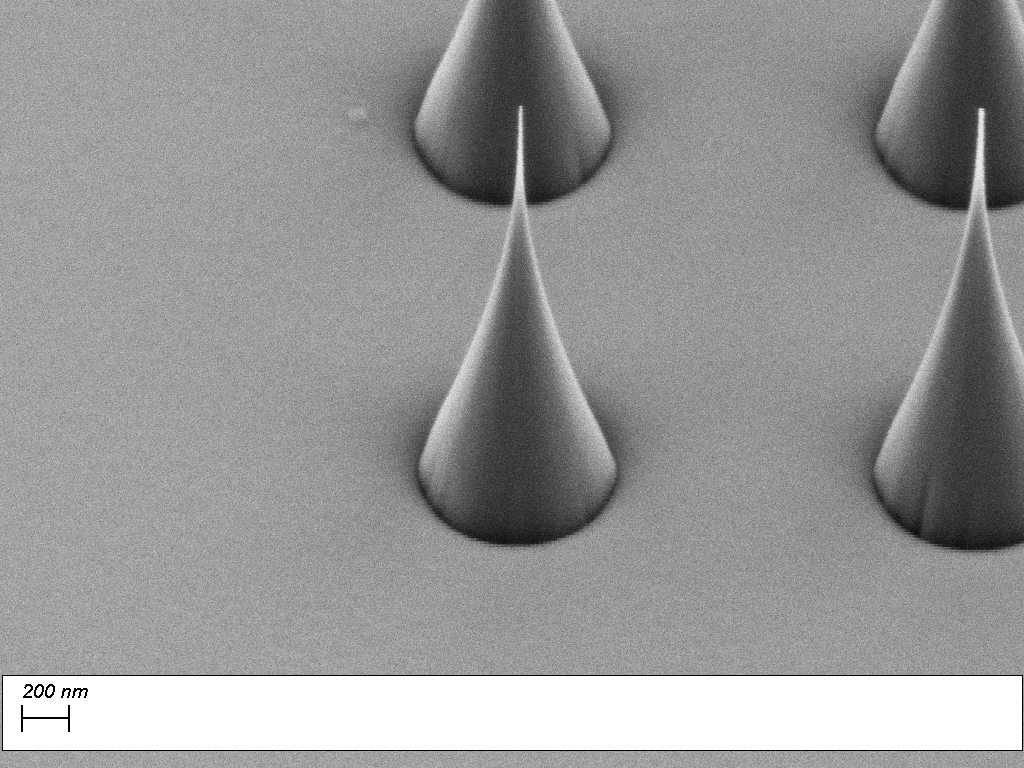
Electron micrograph of silicon carbide tips on a substrate, with a 200 nm scale bar.
A close-up of our SiC nanofabrication. Electron micrograph; scale bar: 200 nm. Select to enlarge.

02 / NANOFABRICATION

Shaping the interaction.

Our team’s research combines electron-beam lithography and dry etching to create SiC nanostructures. We develop the material, mask and etching process around the required dimensions, profile and surface.

Tips, pillars and arrays create different mechanical and optical interactions. Their geometry must suit the sample, surroundings and integration into an experiment.

Read the research methods · SiC resonator fabrication and surface loss
03 / MECHANICAL RESPONSE

Designing mechanical response.

Elastic stiffness and density matter alongside hardness which is why SiC is a suitable material.

For faster AFM measurements, we consider the complete probe together with the instrument’s readout, scanner and force control.

Research on single-crystal 4H-SiC mechanical resonators supports the exploration of compact, high-frequency structures.

04 / RAMAN POLARITONICS

Infrared sensitivity.
Visible-light readout.

Raman polaritonics uses engineered polar-crystal nanostructures to sense nearby materials. Their phonon polaritons—coupled light and crystal vibrations—have a Raman response that changes with their surroundings. This makes changes in the infrared optical environment accessible through visible-light readout.

Patent pending

From a spectral change to a measurement.

Our team’s 2026 preprint reports changes in the Raman response of SiC nanostructures with different surrounding liquids and deposited alumina coatings.

To investigate film thickness or quality, we define the property of interest and compare the optical response with a calibrated reference measurement.

SENSING WINDOWS & PROBES

Research concept

Harsh environments.
Protected optical readout.

We are exploring SiC sensing interfaces that expose nanostructures to a harsh environment while keeping the laser and readout equipment on the protected side.

01 / THE OPTICAL PATH

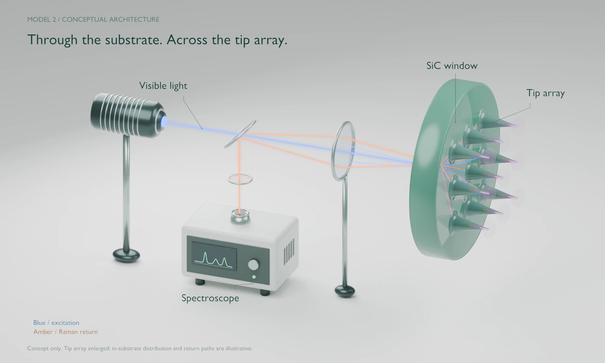
Conceptual angled view of a SiC window with a 3 by 3 sensing-tip array. Blue excitation distributes through the substrate to the tips; amber Raman return passes through the shared lens to a spectroscope.
An array of sensing tips shares one SiC window. Tip dimensions and optical paths are illustrative.

Blue: visible-light excitationAmber: Raman return

1. Illuminate

A lens directs visible laser light through the SiC window from protected Side B to the tip array on exposed Side A.

2. Sense

The field around each tip interacts with nearby material. Changes in that material can alter the Raman response.

3. Collect

Raman-scattered light returns through the SiC and lens to the spectrometer.

02 / THE SENSING SURFACE

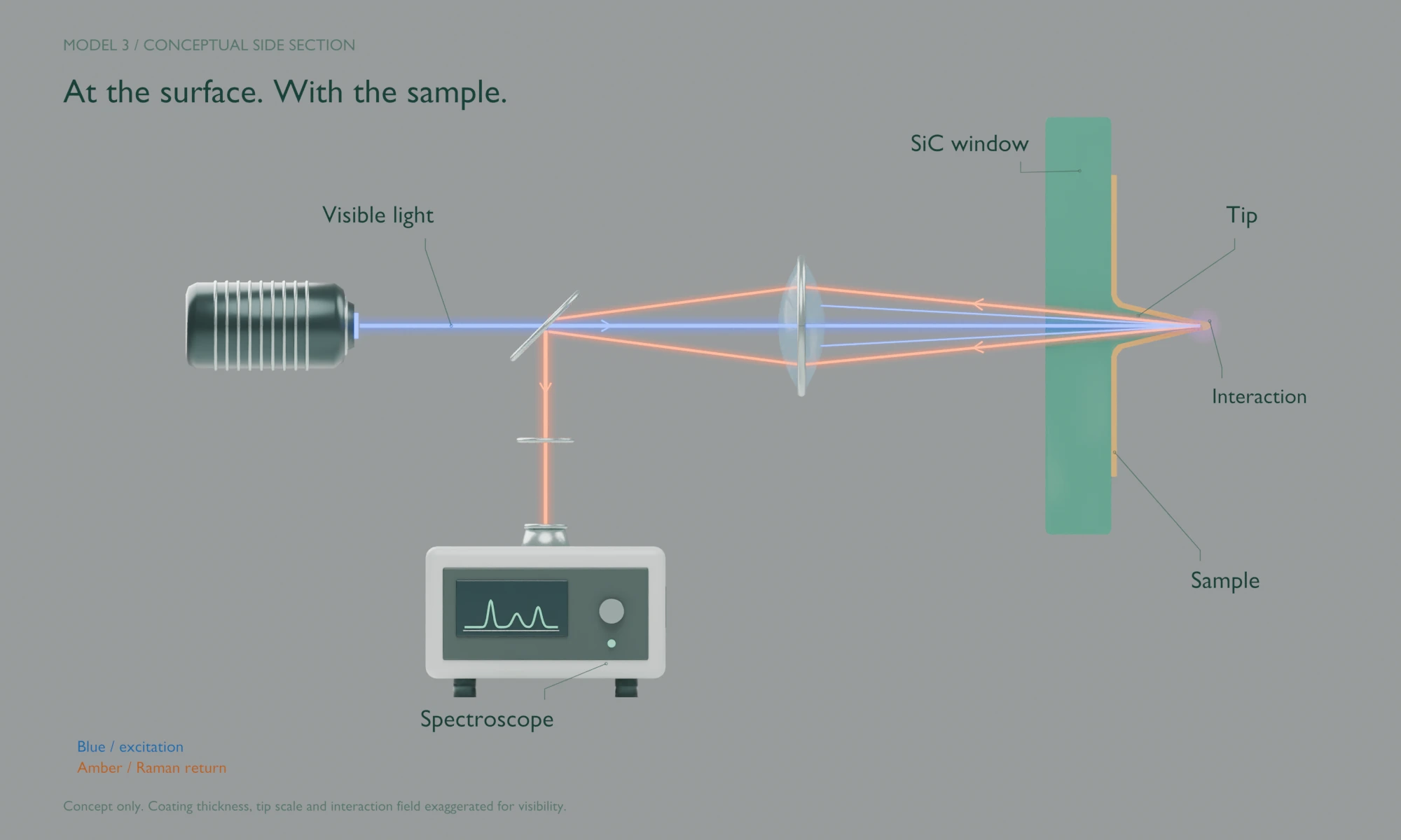
Conceptual side section of a SiC window and tip covered by a thin sample coating, shown in gold. Visible light enters through the window; the local sensing field overlaps the coating, and Raman-scattered light returns to the spectroscope. Coating thickness is exaggerated.
Section detail. Coating thickness and the interaction region are exaggerated for visibility.

A sample at the sensing surface.

The gold-coloured layer represents a thin sample coating over the exposed SiC face and tip. The local sensing field interacts with this coating; Raman-scattered light is collected through the window.

Optical options. Side B can remain unpatterned, as shown. An optional metasurface could be designed to shape illumination or collection.

POSSIBLE FORMATS

Sensing window.

A SiC element mounted in a chamber or process wall could combine an exposed sensing surface with optical access from the protected side.

Insertion probe.

A SiC sensing element could be integrated into a probe, with a protected optical path through the probe to its exposed end.

Tell us what you need to measure, the temperature and chemical environment, and the available optical access.

05 / FROM TECHNOLOGY TO PRODUCTS

Shared foundations.
Different applications.

PolarTip applies our SiC fabrication and mechanical-design expertise to AFM. PolarSense builds on our optical-sensing research. Both rely on precise control of material and geometry.

AFM PROBES / PILOT COLLABORATIONS

PolarTip

PolarTip’s circularly symmetric SiC tips have a measured 5 nm apex radius and high aspect ratio. Pilot discussions focus on feature access, useful tip life and scanning response.

FUTURE PRODUCT / ACTIVE EXPLORATION

PolarSense

PolarSense is an optical-sensing product direction, with thin-film measurement as its first focus. Alongside this work, we are exploring SiC sensing interfaces for harsh environments.

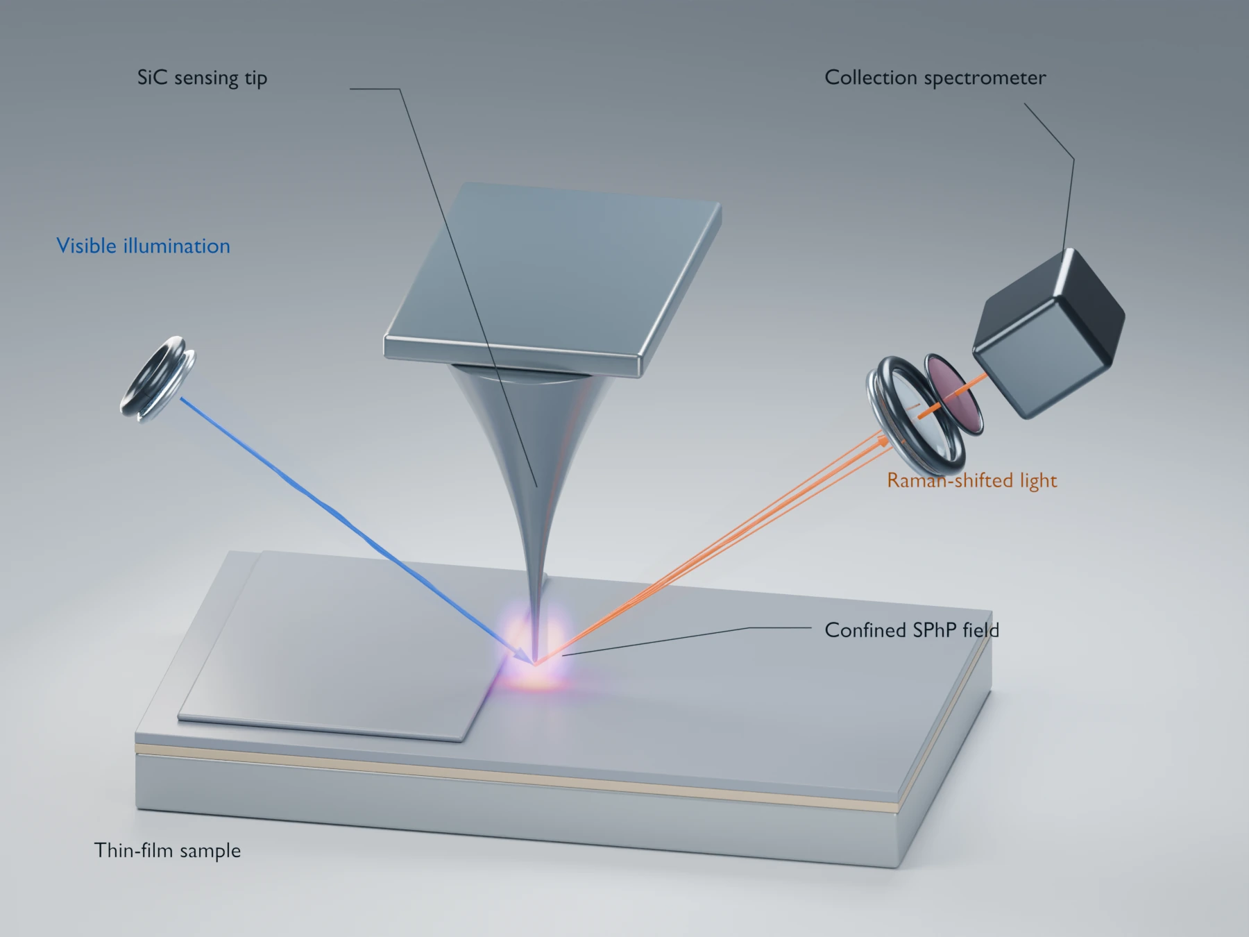
Sharp SiC tip above a layered thin-film sample. A smooth purple–gold near field overlaps the sample surface. Blue illumination reaches the tip–sample region, and amber Raman-shifted light travels through collection optics and a filter to a spectrometer.
The confined sensing field overlaps the film. Raman-scattered light passes through collection optics and a filter to a spectrometer. Conceptual rendering; field shape and extent are illustrative.

SCANNING-PROBE RESEARCH

Optical information alongside topography.

We are investigating how Raman-polaritonic sensing could be combined with a scanning probe to study nearby materials alongside surface topography. This requires a suitable sensing geometry and dedicated optical readout.

06 / RESEARCH

The science behind the work.

RESEARCH FROM OUR TEAM

2026 / ZOGRAF ET AL. / PREPRINT

Research on how SiC nanostructure geometry and the surrounding material influence the Raman response of surface phonon polaritons. Co-authored by Betül Küçüköz and Timur Shegai.

Read our introduction to Raman polaritonics · Meet the team

MATERIAL, PROBE AND OPTICAL LITERATURE

2012 / LANTZ ET AL.

Advanced Functional Materials · SiC layers formed on silicon tips improved wear resistance in the tested conditions. Relevant to material processing and nanoscale contact.

2017 / TANGPATJAROEN ET AL.

ACS Applied Materials & Interfaces · Diamond-tip tests on SiC and silicon surfaces show that relative wear resistance changes with contact size. Material, interface and operating conditions must be considered together.

2025 / HOCHREITER ET AL.

Physical Review Applied · Monolithic 4H-SiC resonators combine high intrinsic quality factors with compact, high-frequency mechanical structures. Supporting research for our mechanical design direction.

2013 / CALDWELL ET AL.

Nano Letters · Demonstrates confined infrared resonances in SiC nanopillars and their observation through visible Raman scattering under suitable conditions. A foundation for our optical-sensing research.

2022 / SCHAEPER ET AL.

ACS Photonics · Demonstrates monolithic SiC metalenses for near-infrared optical control. Supporting research for optional metasurface optics.

Your measurement questions

What makes your technology distinctive?

Our strength is engineering both the SiC structure and the measurement it enables. Geometry can be designed for surface access and mechanical response in AFM, or for an optical interaction with nearby material. Our Raman-polaritonics research adds a distinctive capability: sensitivity to a material’s mid-infrared response, read using visible-light optics.

Why use silicon carbide for these measurements?

SiC combines hardness, stiffness, chemical resistance and thermal stability. These properties support durable probe designs and exploration of demanding measurement environments. Suitable single-crystal SiC also provides optical access through the material. Useful tip life and operating limits depend on the complete structure, sample and instrument.

Can you fabricate structures for a specific measurement?

We develop SiC tips, pillars and arrays around the required interaction. Dimensions, profile and spacing help determine surface access, mechanical response or optical resonance. Our team combines electron-beam lithography, dry etching and measurement design to connect those requirements to a fabrication process and integration plan.

What could you measure in thin films?

Film thickness and changes in optical response are our first targets. Our team’s preprint shows that deposited alumina coatings change the Raman response of SiC nanostructures. We are developing that sensitivity into useful film measurements, calibrated for the material, substrate and sensing geometry—for example, comparing a processed film with a reference.

How could you sense inside a harsh environment?

We are exploring SiC sensing windows and insertion probes that expose the sensing surface to a process while keeping the laser and readout equipment on the protected side. Light passes through suitable SiC to reach the nanostructures and collect their response. The window, interfaces and optical path are developed around the application’s temperature, chemical environment and access constraints.

LET’S TALK

Connect your application
with our research.

Tell us what you need to measure or fabricate and where the current approach falls short. We’ll discuss the technical fit and a useful scope for working together.