AFM PROBES · PILOT COLLABORATIONS

PolarTip

Silicon carbide AFM probes for fine surface features.

Circularly symmetric SiC tips with a measured 5 nm apex radius and a high aspect ratio. Our development focuses on reaching fine surface features, retaining useful tip geometry and enabling faster scanning. 

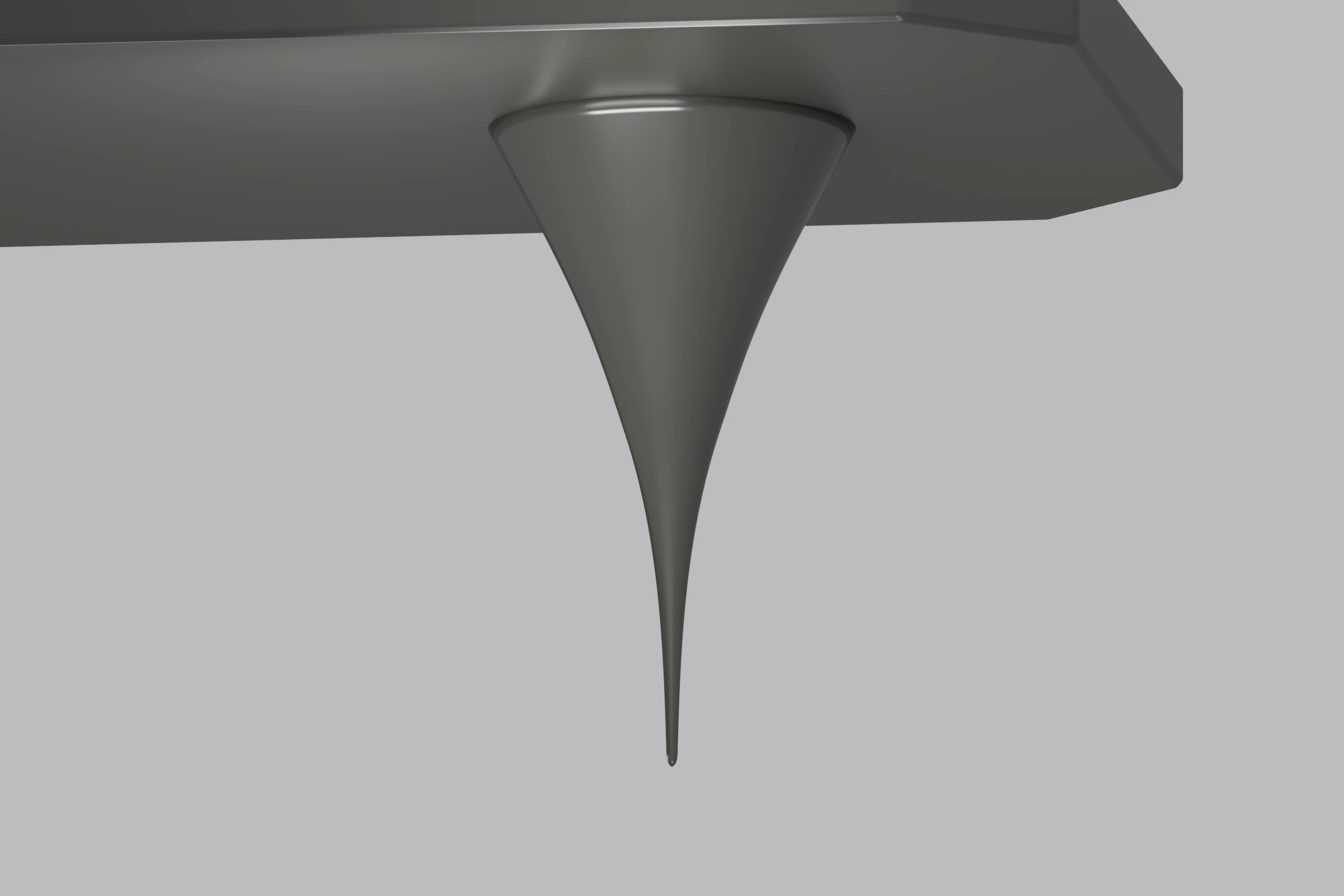
Underside close-up of the SiC tip with a broad curved base, a long slender upper section and a sharp apex beneath the cantilever.
PolarTip tip design · 3D illustration. Select to enlarge.

TIP MATERIAL

SiC

MEASURED APEX RADIUS

5 nm

ASPECT RATIO

High

TIP SHAPE

Circularly
symmetric

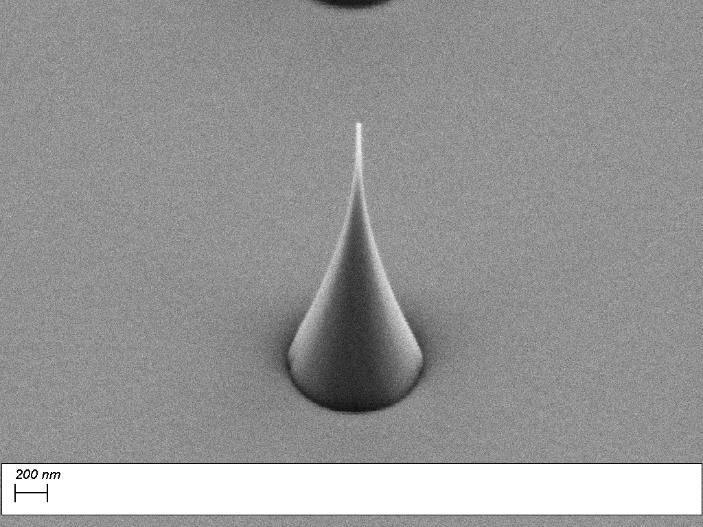
Electron micrograph of a silicon carbide tip on a substrate, with a 200 nm scale bar.
Fabricated SiC tip. Electron micrograph; scale bar: 200 nm. Select to enlarge.

TIP GEOMETRY

A sharp apex.
A consistent profile.

PolarTip’s circularly symmetric tip has the same profile around its axis. Smoothly curved sidewalls taper towards the apex; the high aspect ratio helps the tip access fine, narrow features.

Measured tip curvature

The measured apex radius is 5 nm. The full tip profile, sample and scan settings also influence the detail captured in an AFM image.

Access to the feature

For trenches, pits and closely spaced structures, match the usable tip profile to the opening, depth and sidewall slope.

MEASUREMENT PRIORITIES

Feature access. Probe life.
Faster scanning.

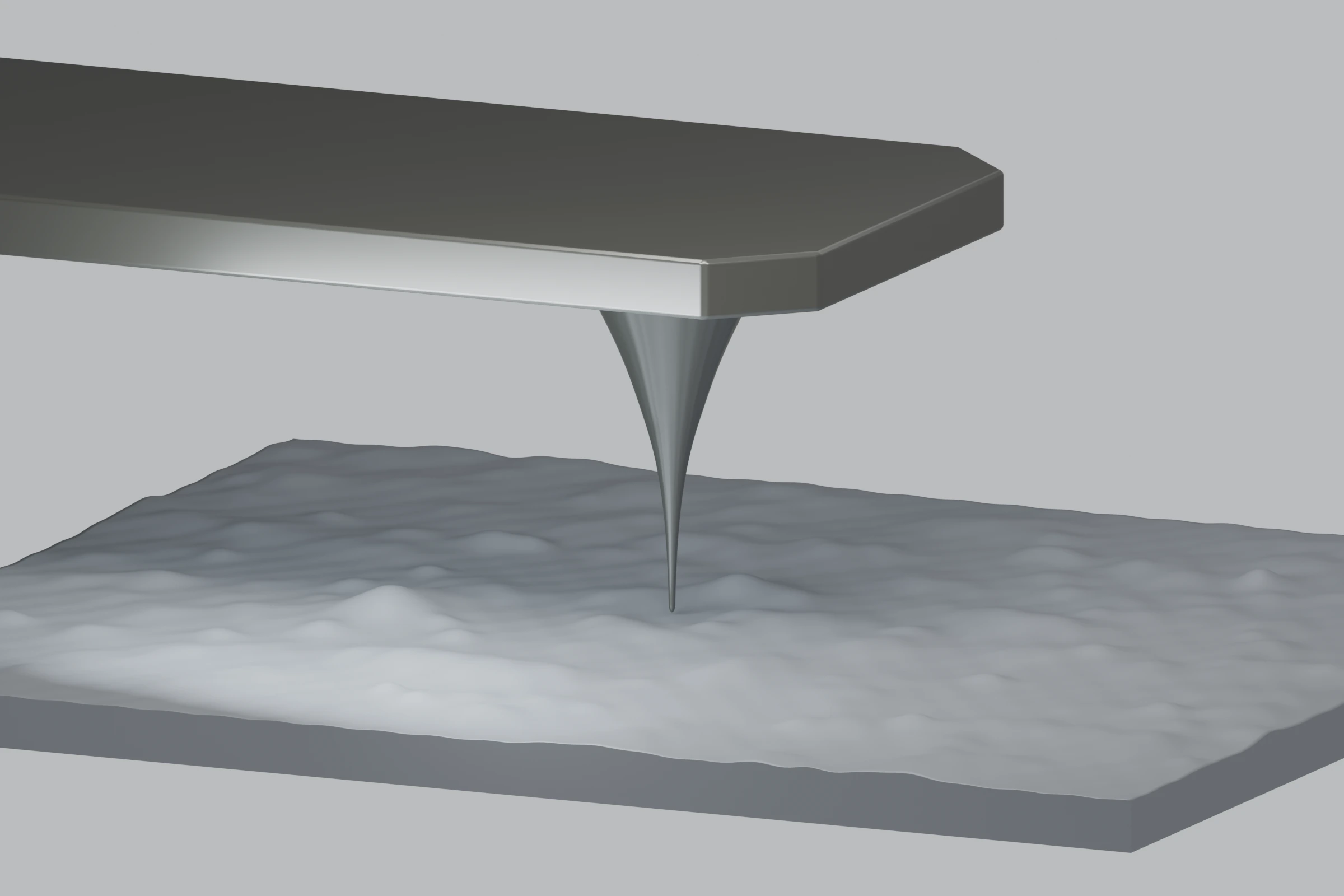
Dark SiC tip above an irregular silver-grey film surface. Conceptual scanning illustration.
Thin-film surface · scanning illustration

01

Preserve detail
through repeated scans

As a tip wears, the surface can appear to change with it. PolarTip’s hard SiC tips are designed to retain their geometry, supporting meaningful comparisons across a measurement series and aiming to reduce interruptions for probe replacement.

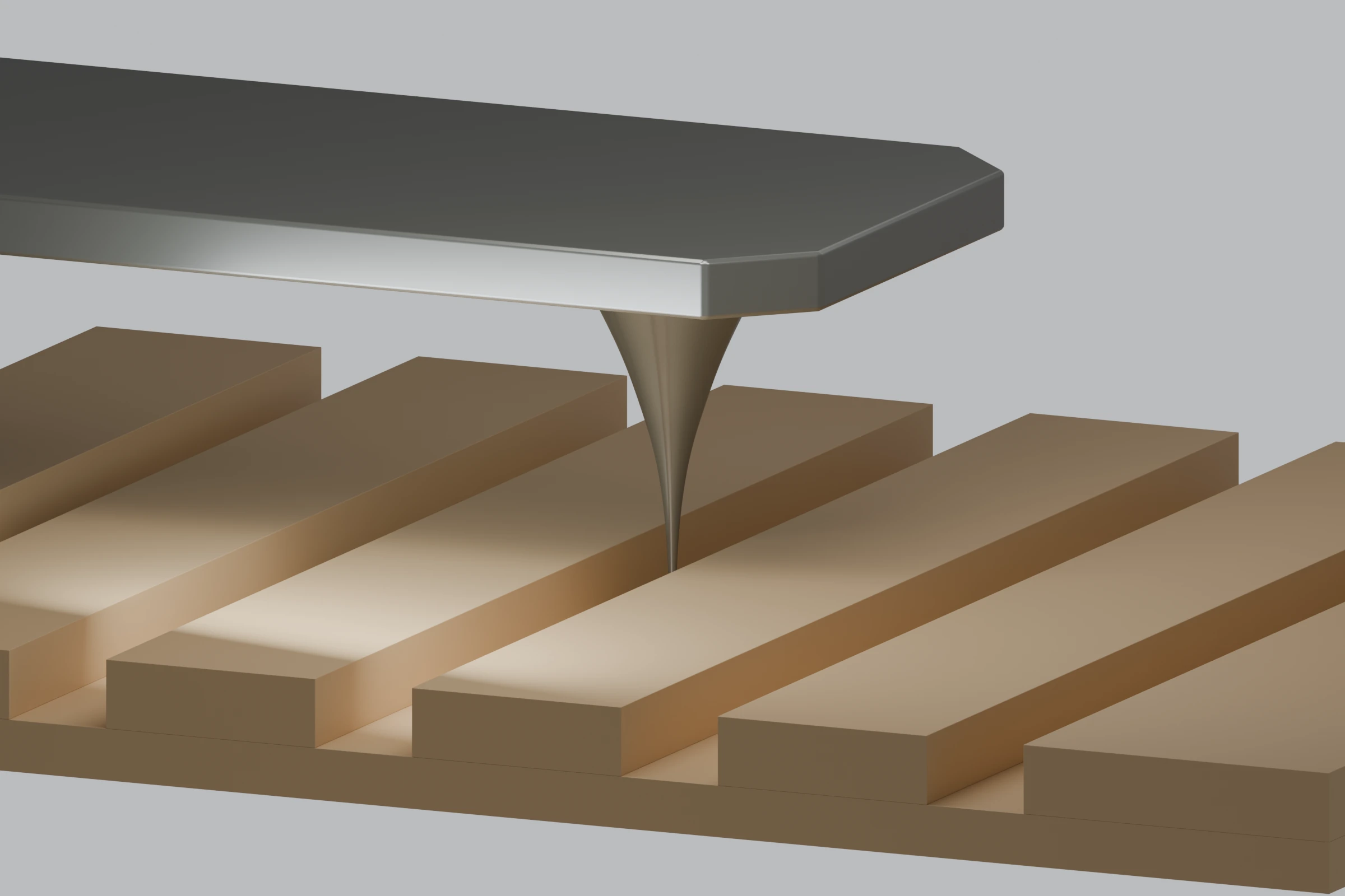
Dark SiC tip positioned within a patterned trench on a warm stone-coloured sample. Conceptual scanning illustration.
Patterned trenches · scanning illustration

02

Reach narrow
surface features

A sharp apex is only useful where the tip can reach. PolarTip’s high aspect ratio and tapered profile are designed for fine, narrow features, with the full geometry determining access to trenches, pits and closely spaced structures.

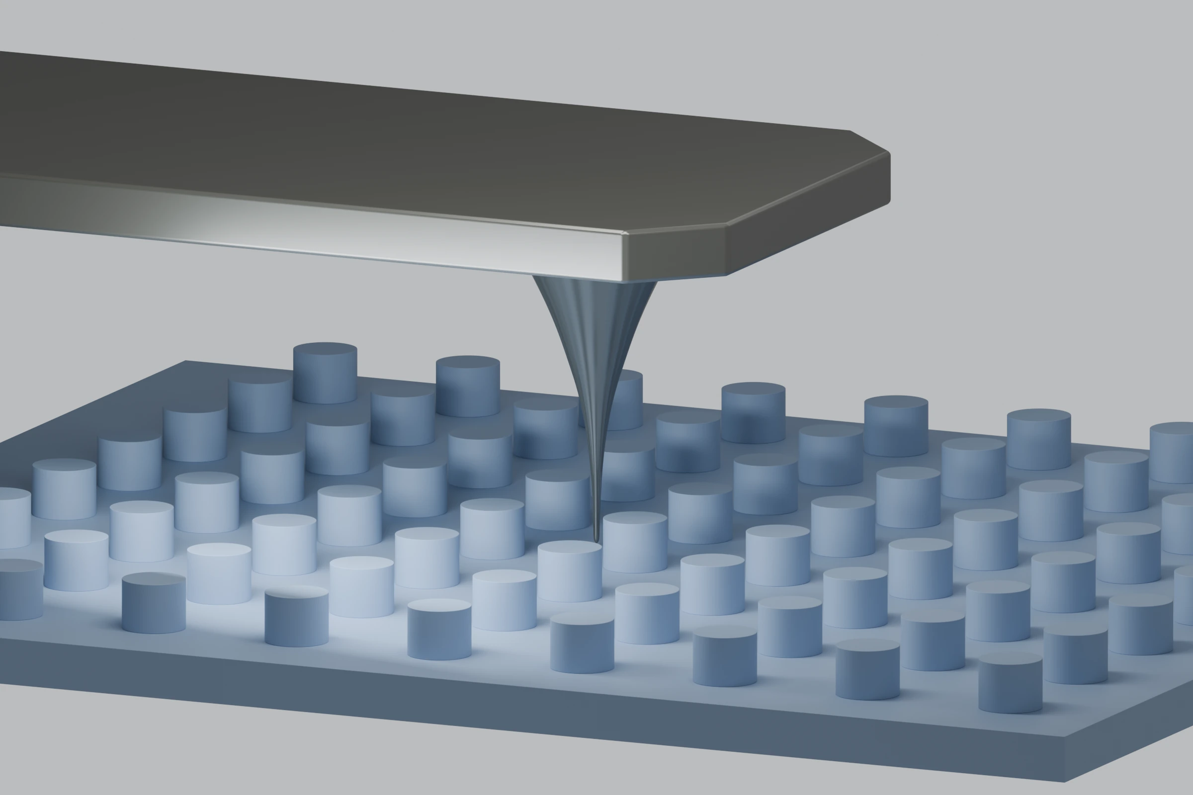
Dark SiC tip between regularly spaced pale blue pillars. Conceptual scanning illustration.
Pillar array · scanning illustration

03

High-throughput
AFM development

Faster scanning can make it practical to examine more locations or compare more samples. We are developing SiC probe configurations for faster response, with performance evaluated alongside the AFM instrument. Together with useful tip life, this is central to our higher-throughput development.

FABRICATION EXPERTISE

Shaped in silicon carbide.

PolarTip brings our nanofabrication expertise to the geometry that connects an AFM instrument with its sample.

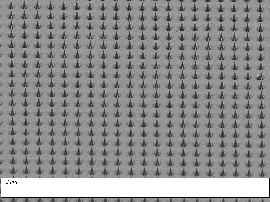
We shape hard SiC into tips designed to retain their geometry through repeated scans. Pilot evaluations assess tip condition and image quality on your sample under agreed operating conditions.

Electron micrograph of an ordered array of silicon carbide tips, with a 2 micrometre scale bar.
Array of fabricated SiC tips. Electron micrograph; scale bar: 2 µm. Select to enlarge.

WORK WITH OUR TEAM

Plan a PolarTip pilot.

Tell us which AFM system you use, what you need to measure and where your current probe limits the work. We’ll discuss the fit, define the probe requirements and agree how to evaluate the result.

A person in cleanroom clothing walking between nanofabrication equipment at Chalmers.
Inside the Chalmers cleanroom.

01

Share the measurement

Start with your AFM model, operating mode and sample. Describe the limitation you want to investigate; an initial outline is enough.

02

Define the evaluation

Discuss instrument fit, probe requirements and a focused comparison of feature access, tip life or scanning response.

03

Agree the practical details

Agree the scope, comparison conditions, responsibilities and next steps before a pilot begins.

RESEARCH DIRECTION

From surface shape
to optical insight.

PolarTip draws on our shared SiC materials and fabrication expertise. Alongside its development, we are exploring optical sensing toward PolarSense, a future product direction with thin-film measurement as its first focus.

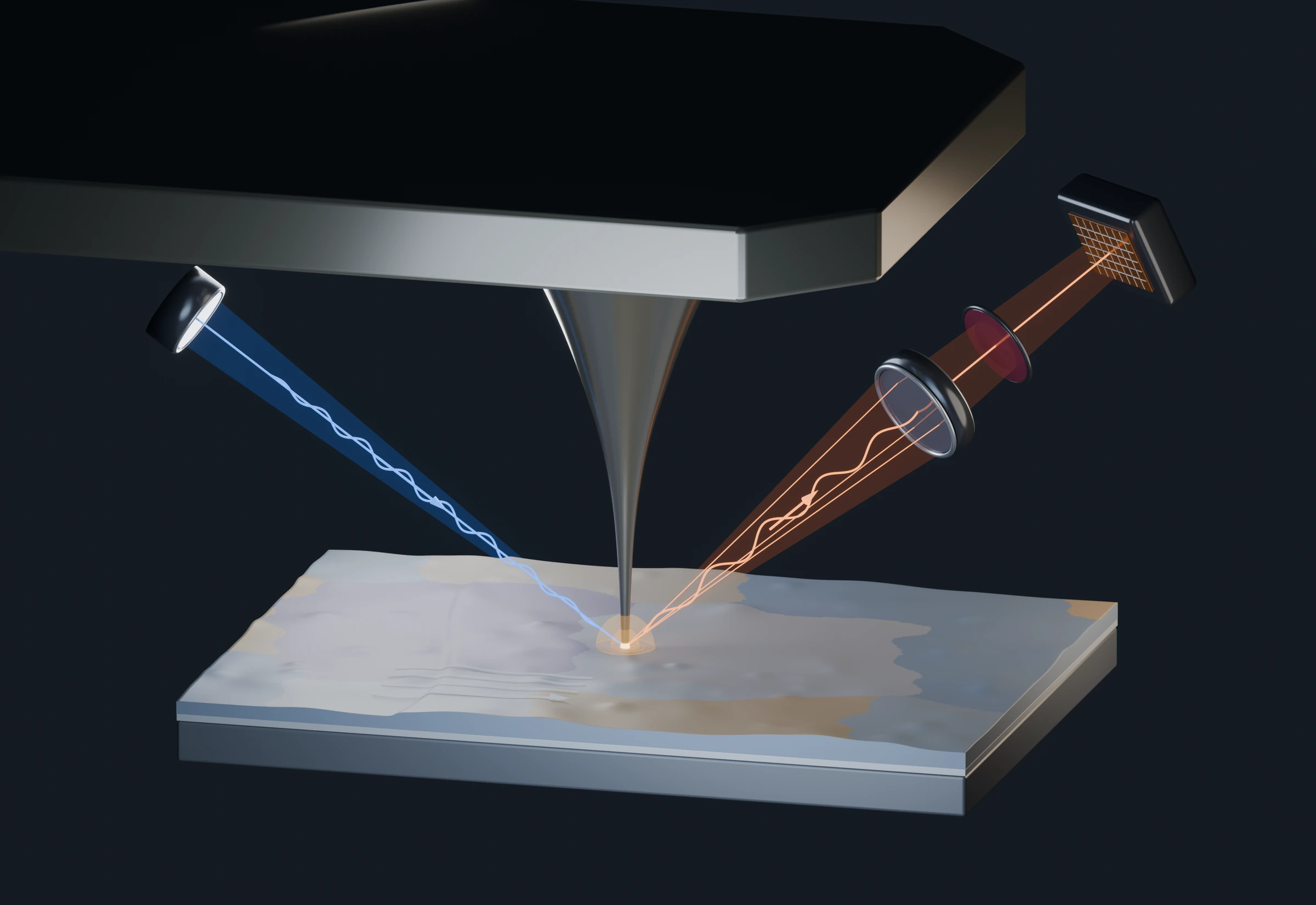
Connecting Raman polaritonics with an AFM probe is a related research direction. It aims to add information about nearby materials to surface topography and requires a suitable sensing geometry, illumination and spectral readout.

AFM-integrated sensing concept: blue illumination reaches the SiC structure near a film; an amber glow marks the conceptual interaction region and orange lines show collection of Raman-scattered light.
AFM-integrated sensing concept. Optical paths and glow are schematic; components are enlarged for clarity.

Before we discuss a pilot

Who are PolarTip pilots for?

Researchers, surface-metrology teams and instrument partners investigating feature access, useful tip life or high-speed AFM development. Start with an application discussion so we can assess the fit and agree a possible evaluation.

What does the measured 5 nm radius mean?

It describes local curvature at the tip’s apex. For your evaluation, we’ll also consider the full tip profile and the dimensions of the features you need to measure.

How would we evaluate useful tip life?

Agree what counts as useful data, then compare image quality and tip condition under matched conditions. Material is one part of the choice; geometry, coatings and operating conditions also matter. Read the tip-life evaluation guide.

Can a pilot include faster scanning or optical sensing?

High-speed AFM is a collaborative development focus, with probe response and instrument compatibility defined together. AFM-integrated optical sensing is a research direction requiring dedicated optics and readout; its scope is discussed separately from the surface-measurement evaluation.
LET’S EXPLORE YOUR APPLICATION

Discuss a
PolarTip pilot.

Start with your sample, AFM system and the measurement you want to improve.